Our Research
Aiming to create and control electromagnetic information in living bodies and in the everyday environment, we carry out research based on magnetic phenomena. We develop sensing systems that capture the electromagnetic fields emitted by living bodies or electrical equipment as information, using the interaction between magnetism and strain or between magnetism and light; new devices based on magnetic phenomena for controlling such fields efficiently; and the nano- and micro-scale magnetic materials needed to realize these devices. The following pages introduce the research we have published so far. For our current research, please contact Prof. Ishiyama or Assoc. Prof. Goto individually, and we will arrange a meeting, including online.
- Near Magnetic Field
- Energy Harvesting
- Strain Sensor
- High-Power Laser
- Spin-Wave IC
- Optical Isolator
- Magnetic Garnet
Near magnetic field measurement
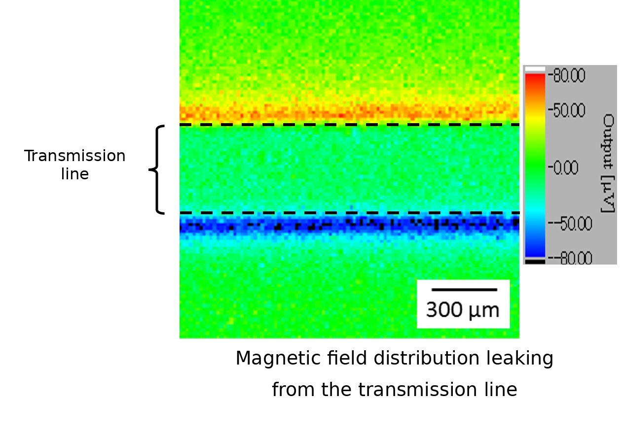
Electronic devices in our daily life use electromagnetic waves of high frequency. Recent progress has made it possible to miniaturize equipment by integrating transmission lines at high density. At the same time, as the lines come closer to each other, the electromagnetic waves leaking from neighboring lines cause harmful interference. This issue, known as electromagnetic compatibility (EMC), remains important as electronic devices continue to spread.
In our laboratory, we apply the magneto-optical effect, the interaction between light and magnetism, to visualize the magnetic field of such leaking electromagnetic waves, aiming to support the further development of electronic devices.
Energy Harvesting
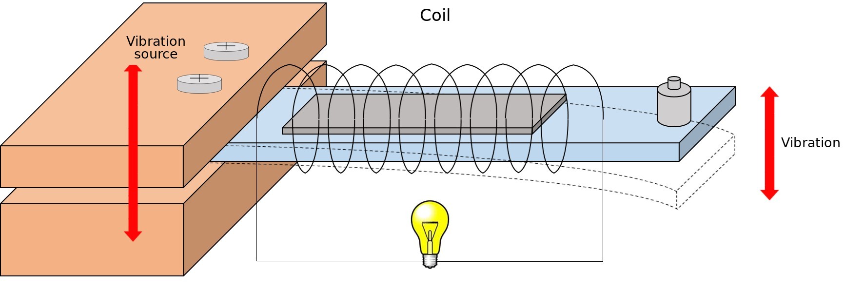
Some magnetic materials, called ferromagnets, are attracted by a magnetic field. When a ferromagnet is magnetized in a magnetic field, it expands or contracts slightly. This phenomenon is called magnetostriction. Conversely, when a force is applied to a ferromagnet, its magnetic properties change; this inverse magnetostriction effect is widely used in sensors.
In our laboratory, we study vibration energy harvesting based on this effect, converting the vibration energy around us, such as that of cars, factory machines, or human walking, into electric power.
The basic structure is a cantilever, in which one end of a narrow strip of magnetostrictive material is fixed and a weight is attached to the free end. When the weight vibrates, the magnetostrictive material expands and contracts, and the magnetization changes through the inverse magnetostriction effect. A coil wound around the material then generates a voltage according to Faraday’s law of induction.
Strain Sensor
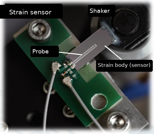
Aging infrastructure such as bridges has become a serious problem, and structural diagnosis is currently carried out by hammering tests performed by human inspectors. As an alternative, monitoring the minute vibrations caused by vehicles passing over a bridge is being studied, which requires highly sensitive vibration sensors.
The impedance of a magnetic material changes when its shape is deformed, an effect known as inverse magnetostriction. In our laboratory, we apply thin-film strain sensors, in which a magnetic film is deposited on a substrate, to vibration sensing.
High-Power Laser
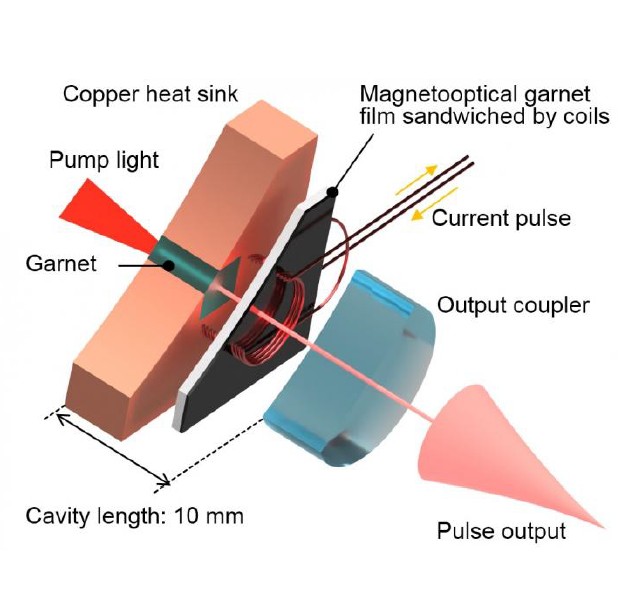
Compact, high-power pulsed lasers are required for laser machining, collision-avoidance sensors in cars, and medical equipment. Q-switches, which generate the pulsed output, have conventionally used electro-optic or acousto-optic elements, but these require thick crystals and large driving circuits, making miniaturization difficult.
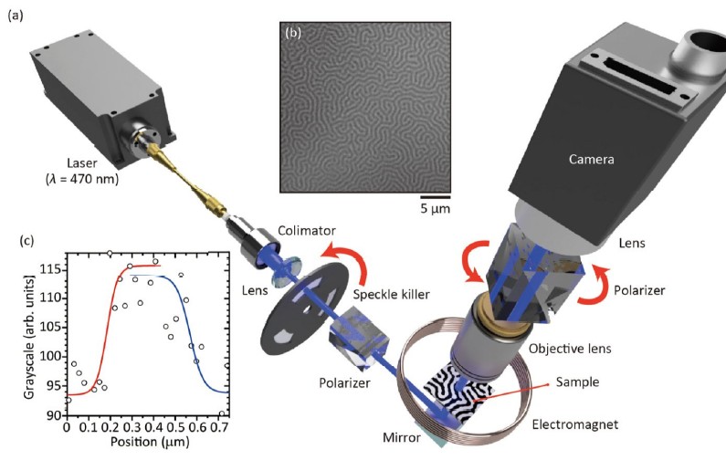
In our laboratory, we realized the world’s first integrable magneto-optical Q-switch using a transparent magnetic garnet film with maze-like magnetic domains. With a compact laser having a cavity length of 10 mm, we achieved a peak power of 1.1 kW and a pulse width of 25 ns. The Q-switch also works for randomly polarized (unpolarized) light, which had been considered difficult, and is expected to make lasers smaller and less expensive.
Spin-Wave IC

Semiconductor circuits carry information with electric current, so heat generation becomes a serious problem as devices are scaled down. In our laboratory, we aim to realize integrated circuits (spin-wave ICs) that process information without electric current, using spin waves, the waves propagating in magnetic materials.
We have developed a phase interferometer that reduces the propagation loss to one hundredth by combining a magnetic garnet, a magnetic insulator, with gold films. Using Ψ-shaped waveguides, we then demonstrated NAND and NOR operations working in the GHz range for the first time in the world. We have also created frequency bands that reflect spin waves using two-dimensional magnonic crystals, in which small copper disks are arranged in a hexagonal pattern, and have shown that spin waves can propagate through a Z-shaped waveguide with more than 5,000 times the intensity of conventional waveguides.
Optical Isolator

Optical signals carry the information of the internet, and optical isolators, which block light reflected back into the circuit, are indispensable. However, magnetic garnet, the high-performance magneto-optical material, cannot be grown directly on a silicon substrate and required a bonding process, so its integration with photonic circuits had long been a challenge.
In our laboratory, we developed laser annealing, which heats only the required area with laser light, and made it possible to crystallize magnetic garnet without damaging electrodes or photonic circuits. Using this technique, we demonstrated the world’s first optical isolator integrated directly on a silicon photonic circuit. We also developed a nanocomposite magnetic garnet film, in which cerium oxide nanoparticles are dispersed, achieving a magneto-optical figure of merit of 510°/dB, about four times that of conventional polycrystalline films.
Magnetic Garnet
The performance of magneto-optical and spin-wave devices is determined by the quality of the magnetic garnet films at their heart, so our laboratory develops materials as well as devices. We fabricate both polycrystalline and single-crystal films, with experience in magnetron sputtering (MS), ion beam sputtering (IBS), pulsed laser deposition (PLD), and liquid phase epitaxy (LPE). At present we focus on ion beam sputtering, which has yielded a large perpendicular magnetic anisotropy. Recently we have shown that perpendicular magnetic anisotropy is obtained even on substrates with different lattice constants, and clarified that its origin is growth-induced magnetic anisotropy, which allows material design free from the choice of substrate.
| Representative garnet films | Method | Press |
|---|---|---|
| Polycrystalline Ce:YIG | IBS | Press |
| Single-crystal Ce:YIG | IBS | Press 1Press 2Press 3 |
| Laser-annealed polycrystalline Ce:YIG | IBS | Press 1Press 2 |
| Single-crystal YIG | PLD | Press |
| Single-crystal YIG | LPE | Press 1Press 2Press 3Press 4Press 5Press 6 |